The story of this amplifier starts back in 2017 when I held a FCC Part 5 experimental license (WI2XTC). This was prior to FCC granting amateur privileges on 2200 and 630 meters. I was looking for a kilowatt-class amplifier that seemed reasonably easy and inexpensive to reproduce. I settled on the W1VD kilowatt class D design.
After building the amplifier I had a lot of problems with blown FETs. After many months of testing, troubleshooting and trying various things, I got that problem under control for the most part. It turns out this was not a problem with the design or my construction, but simply that modern modes and operating practices are not consistent with the intent of the design. The amplifier was designed for a steady RF signal at its input, with transmission to start and stop by using one of the keying inputs to enable and disable the FET driver IC. That just isn’t how modern computer generated modes work. The software usually provides for PTT (amplifier keying), but it is the opposite of what would be needed to keep the amplifier happy. PTT is asserted before RF generation starts and held until after RF stops. The amplifier needed the opposite to be safe: PTT asserted after the start of RF generation and released before RF stops.
Initially I was experiencing frequent FET failures with any exciter I used, but they were far more common, in fact almost guaranteed using an exciter capable of amplitude shaping the start and/or end of the RF envelope. I don’t have a storage oscilloscope, but after seeing some FET drain waveforms provided by other users of the same amplifier it was apparent there were (or could be) voltage spikes exceeding the 200 volt rating of the FQP34N20 FETs at the start and especially end of a transmission. Additionally there appeared to be extended times of zero voltage on one pair of FETs or the other, possibly indicating a longer than normal on time. One might wonder if there were current surges occurring at those times. After a lengthy search for replacement FETs rated for higher voltage and current but otherwise having similar ratings to the FQP34N20, I tried the FDA59N30. That eliminated any blowing of FETs with exciters or modes that are not capable of RF envelope shaping, such as the QRP Labs Ultimate 3S which I use extensively. I had just one FET failure in more than a year of operation. It appeared that may have been due to overheating. I found the mounting screw on the failed FET was not tight. Both the mounting surface of the FET and the Sil-Pad underneath were discolored in a way that suggested excessive heating. The FDA59N30 is a current production part while the FQP34N20 is long discontinued and becoming very hard to find except from some overseas sources which are selling counterfeit devices.
During the summer of 2020 I was invited to join the early testing team for the new FST4 and FST4W modes being developed for use at LF and MF. It was one of the better things to happen in 2020! Initially I was able to run these modes using the phasing exciter but I noticed some peculiar glitches on the scopematch (sophisticated RF power and SWR monitor using an oscilloscope) at the start and particularly at the end of transmissions. I also had some intermittent problems with amplitude and phase fluctuations during FST4/W transmissions. Eventually while looking for the source of that problem, I discovered the IR2110 FET driver was not entirely healthy. One side was OK but the other was providing only weak gate drive to the FETs. I replaced the driver and that was the end of being able to transmit using the new modes! FETs were constantly meeting their demise with the new modes, while other modes were OK. My pile of dead FETs was again growing rapidly! At about the same time I learned something about the new modes that I had not previously known. They were intentionally using envelope shaping at the beginning and end of transmissions! (Note: with the general availability release of WSJT-X 2.3.0, the FST4/W envelope shaping can be disabled.) Sure enough, when I tried manually enabling the FET driver after the envelope shaping at the start and disabling it before RF shaping commenced at the end of transmissions, FETs did not fail.
It has never been clear to me exactly where in the amplifier problems start with non-constant amplitude drive, but clearly bad things were happening somewhere. Was it strictly in the output circuit, or was something going wrong in the driver or the pre-driver logic? It would be fair to say I was never entirely happy with the configuration of the amplifier anyway. Since it used a flip-flop to clock the IR2110 FET driver, it required the RF input signal to be at twice the operating frequency. For 137.5 kHz operation, it needed RF drive at 275 kHz. In order to achieve that with common exciters and relatively minimum hassle, I used a frequency doubler circuit before the driver. That always seemed like unnecessary complexity to me, but at the time of construction there were few, if any alternate driver designs for class D amplifiers that didn’t use a flip-flop, therefore requiring drive at twice the operating frequency. The doubler also caused some problems running EbNaut, which uses 180 degree phase shift keying.
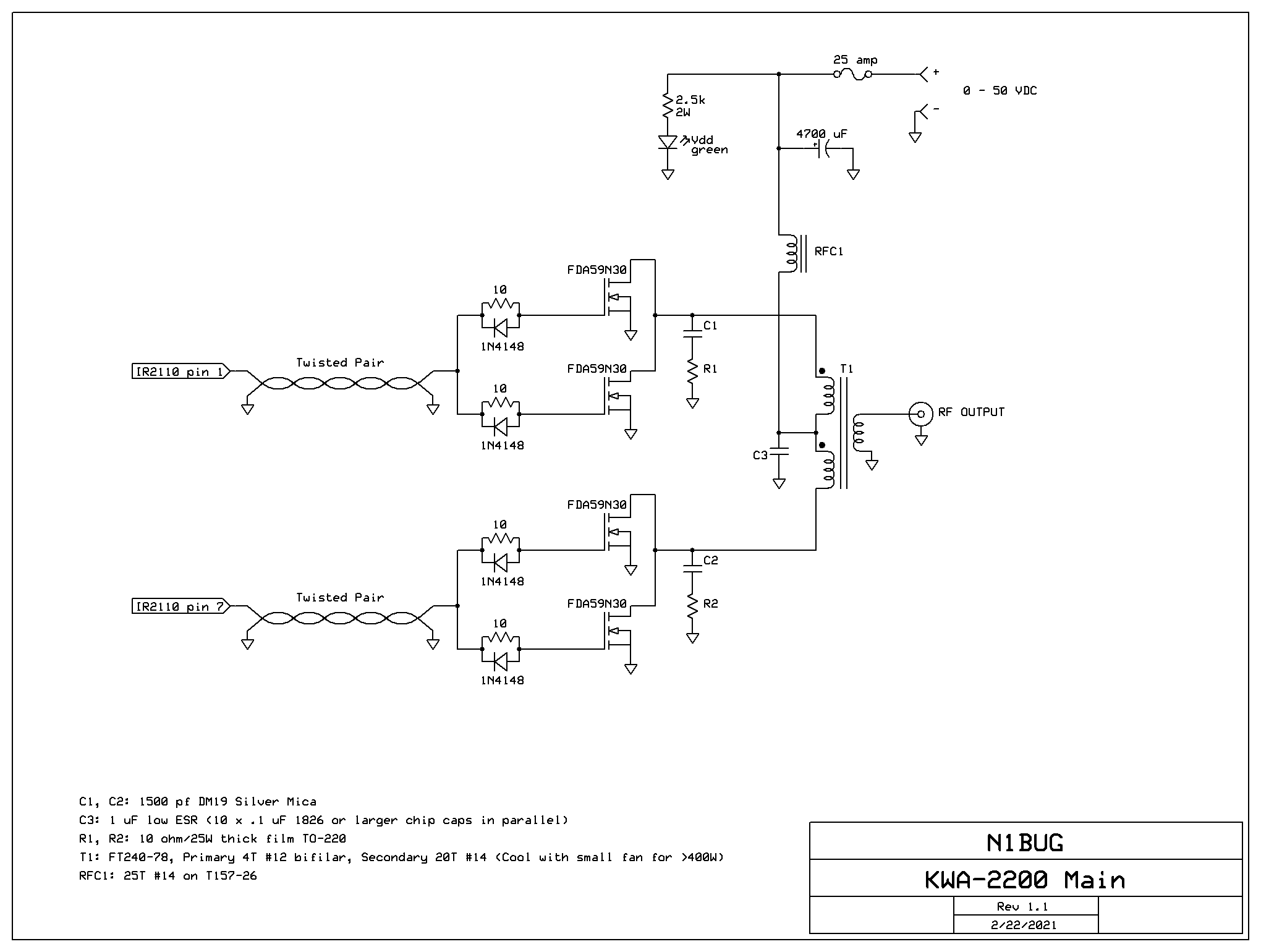
While struggling to think of a solution to the FST4/W envelope shaping killing FETs en masse, it came to my attention that others were now using drivers for class D amplifiers that did not use the flip-flop and worked with “normal” drive at the operating frequency. I decided to try an experiment. Melding elements from three different designs, I came up with a driver that provided all of the control inputs of the original, required no doubler and allowed for some adjustment of the duty cycle. The circuit uses a 1:9 impedance step up transformer driving a pair of LM311 comparators. The comparator outputs control the IR2110 FET driver. One obvious advantage is that this does not require drive at twice the operating frequency. Another is that, unlike the original driver configuration this one allows for some adjustment of the length of the drive pulses to the FETs. This made it possible to get cleaner drain waveforms with less high frequency ringing.
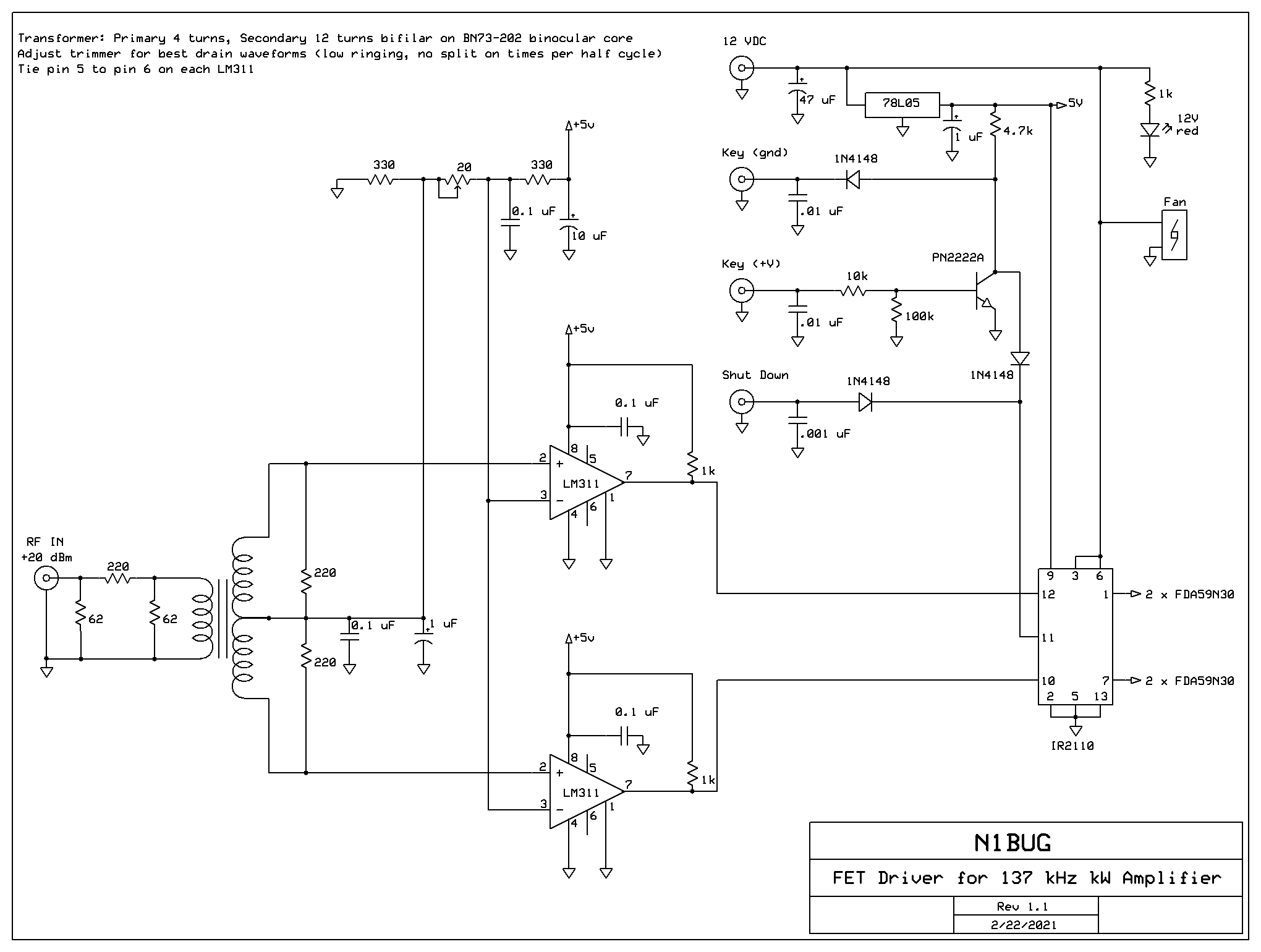
With the original driver there was always some high frequency drain ringing. With this driver it can be almost entirely eliminated by adjusting the 20 ohm trimmer to vary the duty cycle or length of drive pulses. There is a tradeoff between the circuits. The original amplifier input consisted of a frequency doubler and the flip-flop preceding the IR2110. With that configuration there was little to no change in drain waveforms over a 15 dB drive power range. With the new circuit, drain waveforms change with drive level. The change is minimal over about a 6 dB range but increases outside those limits. The range of acceptable input can be pushed to 15 dB before things start looking really alarming. This worked fine for all but FST4/W modes (prior to the 2.3.0 GA release with envelope shaping disabled). With FST4/W slowly rising from zero to full power at the start of a transmission and slowly decreasing from full power to zero at the end, the drain waveforms went through some ugly periods. I was still occasionally losing FETs.
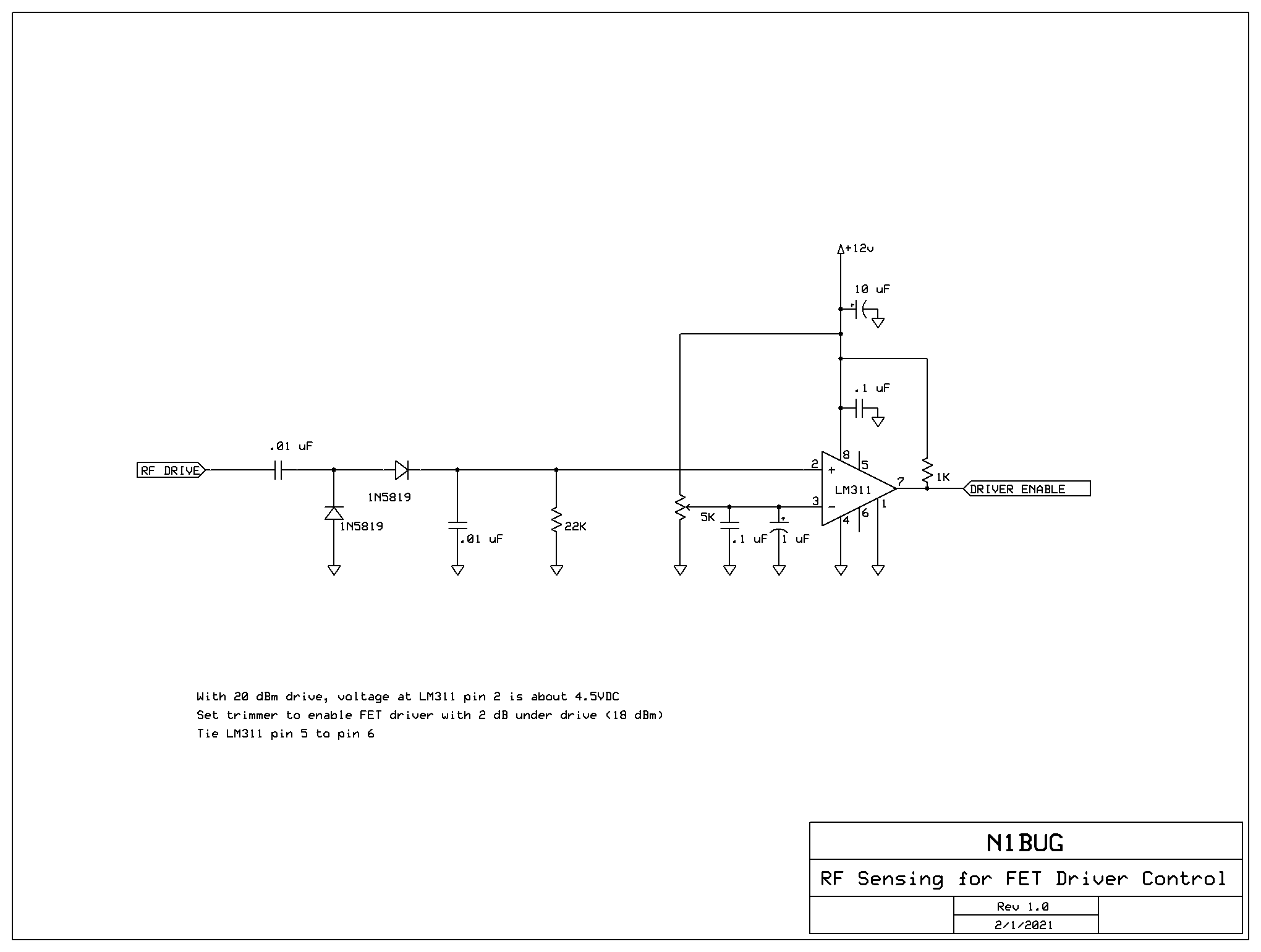
I wondered if an RF sensing circuit could solve that problem. It should be possible to sample the incoming RF drive, rectify it and use the resulting DC voltage to control a comparator which would enable the IR2110 only after drive had reached a safe amplitude. The question I had was would it be fast enough to disable the FET driver at the end while the envelope was decaying. If it was too slow, it might not disable the driver before the amplitude reached a low enough level to cause problems. Never blindly trust my math or circuit design skills but by my reasoning it looked possible. The envelope shaping occurs over approximately 2.5 seconds for a FST4/W 1800 second transmission. I believe it scales linearly with the T/R period, so for the 15 second transmission it should be about .02 second. There should be plenty of time to shut things down if I used an RC time constant of about .0002 second. Instead of rambling though all of my rough calculations let me just say I tested the circuit as built with several hours of FST4-15 transmissions, which would require the fastest timing. There were no glitches evident and no FETs were harmed during the test.
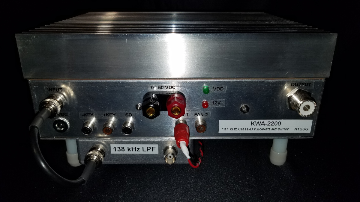
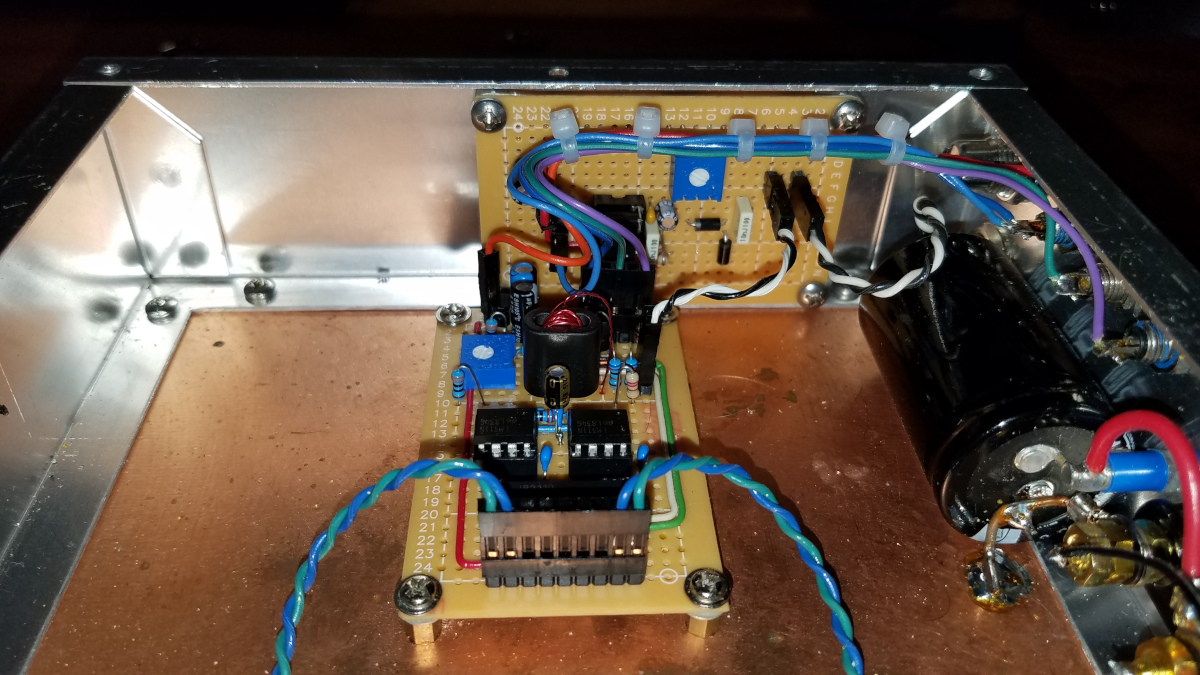
I built the new driver circuit on a board which was the same size as the original and used the same connectors, so it was a drop in replacement for the amplifier. Similarly the RF sensing and control circuit is a drop in replacement for the no longer needed frequency doubler.
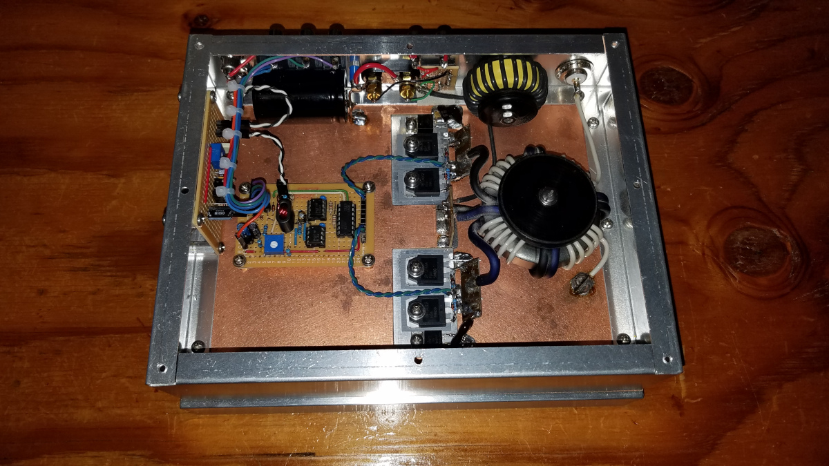
The remainder of the amplifier remains mostly unchanged from the W1VD circuit except for the substitution of FETs as discussed earlier. It should be noted that for power levels above 400 to 500 watts at high duty cycle, a small fan cooling the output transformer is a good idea.
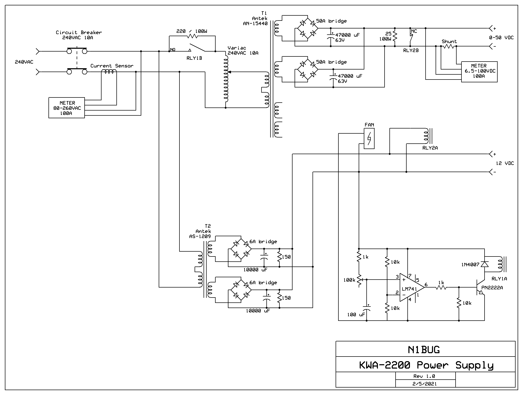
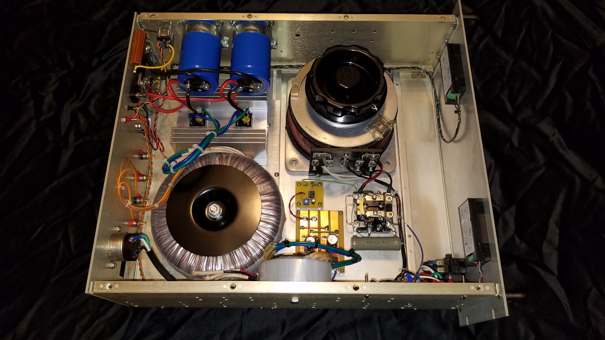
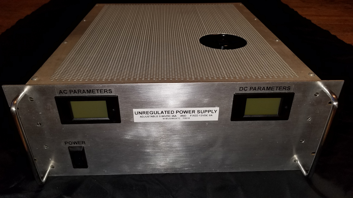
The power supply is about as simple (and efficient) as you can get, a few luxuries notwithstanding. It is unregulated, consisting of a variac, transformer, two bridge rectifiers and two large filter capacitors. It can provide 0 to 50 volts for the FET drains. The power transformer has two secondaries. Each has its own rectifier and filter capacitor. The two are combined at the output terminals of the supply. A small fan is used to blow air across the bridge rectifiers to aid in cooling. Because the filter capacitors are large and the transformer resistance is low, a soft start circuit is used to prevent inrush current problems. There is a separate transformer with a similar configuration to supply 12 volts to the amplifier driver circuits. The 12 volt supply also controls the soft start by means of a comparator which closes a relay to short out a resistor in the AC input to the variac after a short (adjustable) delay.